


ESAI Programming Model
DSP56366 24-Bit Digital Signal Processor User Manual, Rev. 4
8-26 Freescale Semiconductor
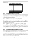
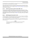
8.3.3.10 RCCR Receiver High Frequency Clock Direction (RHCKD) - Bit 23
The Receiver High Frequency Clock Direction (RHCKD) bit selects the source of the receiver high
frequency clock when in the asynchronous mode (SYN=0), and the IF2/OF2 flag direction in the
synchronous mode (SYN=1).
In the asynchronous mode when RHCKD is set, the internal clock generator becomes the source of the
receiver high frequency clock, and is the output on the HCKR pin. In the asynchronous mode when
RHCKD is cleared, the receiver high frequency clock source is external; the internal clock generator is
disconnected from the HCKR pin, and an external clock source may drive this pin.
When RHCKD is cleared, HCKR is an input; when RHCKD is set, HCKR is an output.
In the synchronous mode when RHCKD is set, the HCKR pin becomes the OF2 output flag. If RHCKD
is cleared, then the HCKR pin becomes the IF2 input flag. See Table 8-1 and Table 8-9.
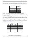
8.3.4 ESAI Receive Control Register (RCR)
The read/write Receive Control Register (RCR) controls the ESAI receiver section. Interrupt enable bits
for the receivers are provided in this control register. The receivers are enabled in this register (0,1,2 or 3
receivers can be enabled) if the input data pin is not used by a transmitter. Operating modes are also
selected in this register.
Hardware and software reset clear all the bits in the RCR register.
The ESAI RCR bits are described in the following paragraphs.
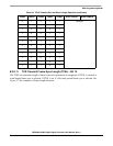
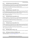
Table 8-9 HCKR Pin Definition Table
Control Bits
HCKR PIN
SYN RHCKD
0 0 HCKR input
0 1 HCKR output
10 IF2
11OF2
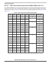
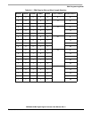
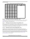
11109876543210
X:$FFFFB7 RSWS1 RSWS0 RMOD RMOD RWA RSHFD
RE3 RE2 RE1 RE0
23 22 21 20 19 18 17 16 15 14 13 12
RLIE RIE REDIE REIE RPR
RFSR RFSL RSWS4 RSWS3 RSWS2
Reserved bit - read as zero; should be written with zero for future compatibility.
Figure 8-9 RCR Register