


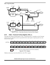

ESAI_1 Programming Model
DSP56366 24-Bit Digital Signal Processor User Manual, Rev. 4
9-4 Freescale Semiconductor
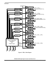
9.2.6 Serial Transmit 5/Receive 0 Data Pin (SDO5_1/SDI0_1)
SDO5_1/SDI0_1 transmits data from the TX5_1 serial transmit shift register when programmed as
transmitter pin, or receives serial data to the RX0_1 serial shift register when programmed as a receiver
pin. SDO5_1/SDI0_1 may be programmed as a general-purpose pin (PE6) when the ESAI_1 SDO5_1 and
SDI0_1 functions are not being used.
9.2.7 Receiver Serial Clock (SCKR_1)
SCKR_1 is a bidirectional pin that provides the receivers serial bit clock for the ESAI_1 interface.
SCKR_1 may be programmed as a general-purpose I/O pin (PE0) when the ESAI_1 SCKR_1 function is
not being used.
9.2.8 Transmitter Serial Clock (SCKT_1)
SCKT_1 is a bidirectional pin that provides the transmitters serial bit clock for the ESAI_1 interface.
SCKT_1 may be programmed as a general-purpose I/O pin (PE3) when the ESAI_1 SCKT_1 function is
not being used.
9.2.9 Frame Sync for Receiver (FSR_1)
The FSR_1 pin is a bidirectional pin that provides the receivers frame sync signal for the ESAI_1 interface.
FSR_1 may be programmed as a general-purpose I/O pin (PE1) when the ESAI_1 FSR_1 function is not
being used.
9.2.10 Frame Sync for Transmitter (FST_1)
The FST_1 pin is a bidirectional pin that provides the transmitters frame sync signal for the ESAI_1
interface. FST_1 may be programmed as a general-purpose I/O pin (PE4) when the ESAI_1 FST_1
function is not being used.
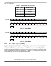
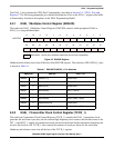
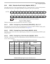
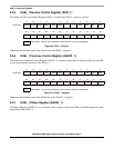
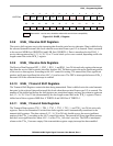
9.3 ESAI_1 Programming Model
The ESAI_1 has the following registers:
• One multiplex control register
• Five control registers
• One status register
• Six transmit data registers
• Four receive data registers
• Two transmit slot mask registers
• Two receive slot mask registers
• One special-purpose time slot register