


Power
DSP56366 24-Bit Digital Signal Processor User Manual, Rev. 4
Freescale Semiconductor 2-3
2.2 Power
2.3 Ground
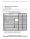
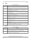
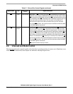
Table 2-2 Power Inputs
Power Name Description
V
CCP
PLL Power — V
CCP
is V
CC
dedicated for PLL use. The voltage should be well-regulated and the input
should be provided with an extremely low impedance path to the V
CC
power rail. There is one V
CCP
input.
V
CCQL
(4) Quiet Core (Low) Power — V
CCQL
is an isolated power for the internal processing logic. This input
must be tied externally to all other chip power inputs. The user must provide adequate external
decoupling capacitors. There are four V
CCQL
inputs.
V
CCQH
(3) Quiet External (High) Power — V
CCQH
is a quiet power source for I/O lines. This input must be tied
externally to all other chip power inputs. The user must provide adequate decoupling capacitors. There
are three V
CCQH
inputs.
V
CCA
(3) Address Bus Power — V
CCA
is an isolated power for sections of the address bus I/O drivers. This input
must be tied externally to all other chip power inputs. The user must provide adequate external
decoupling capacitors. There are three V
CCA
inputs.
V
CCD
(4) Data Bus Power — V
CCD
is an isolated power for sections of the data bus I/O drivers. This input must
be tied externally to all other chip power inputs. The user must provide adequate external decoupling
capacitors. There are four V
CCD
inputs.
V
CCC
(2) Bus Control Power — V
CCC
is an isolated power for the bus control I/O drivers. This input must be tied
externally to all other chip power inputs. The user must provide adequate external decoupling
capacitors. There are two V
CCC
inputs.
V
CCH
Host Power — V
CCH
is an isolated power for the HDI08 I/O drivers. This input must be tied externally
to all other chip power inputs. The user must provide adequate external decoupling capacitors. There
is one V
CCH
input.
V
CCS
(2) SHI, ESAI, ESAI_1, DAX and Timer Power — V
CCS
is an isolated power for the SHI, ESAI, ESAI_1,
DAX and Timer. This input must be tied externally to all other chip power inputs. The user must provide
adequate external decoupling capacitors. There are two V
CCS
inputs.
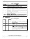
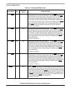
Table 2-3 Grounds
Ground Name Description
GND
P
PLL Ground — GND
P
is a ground dedicated for PLL use. The connection should be provided with an
extremely low-impedance path to ground. V
CCP
should be bypassed to GND
P
by a 0.47 µF capacitor
located as close as possible to the chip package. There is one GND
P
connection.
GND
Q
(4) Quiet Ground — GND
Q
is an isolated ground for the internal processing logic. This connection must
be tied externally to all other chip ground connections. The user must provide adequate external
decoupling capacitors. There are four GND
Q
connections.