


15 - 60
15. ABSOLUTE POSITION DETECTION SYSTEM
(4) Differences between A1SD75 (AD75) and A1SD71 (AD71)
The sequence programs shown in (2) of this section differ from those for the A1SD71 (AD71) in the
following portions. 1) to 20) in the following sentences indicate the numbers in the programs given in
(2) of this section.
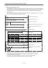
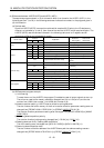
(a) Devices used
Since the A1SD75 (AD75) is a one-slot module which occupies 32 I/O points, the I/O devices are
different, as indicated by 1) and 2), from those of the two-slot A1SD71 which occupies 48 point. The
A1SD75 (AD75) uses the devices indicated in the following table, and its D registers and M
contacts are different as indicated by 3) and 4).
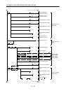
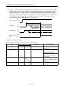
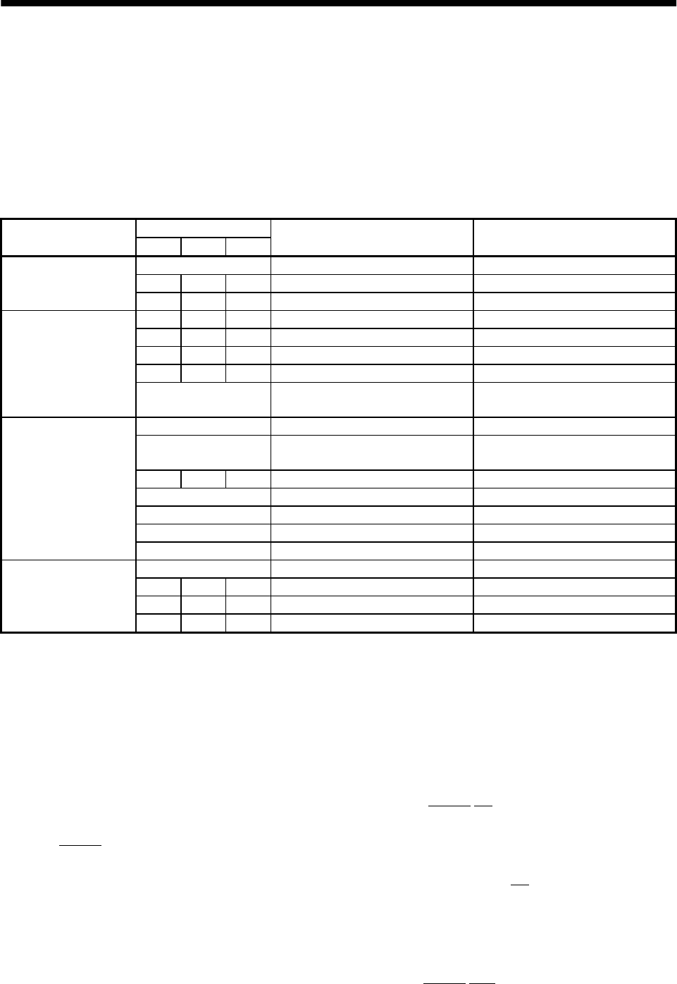
Devices
Device name
Axis 1 Axis 2 Axis 3
Application
Bit device :Data at ON
Data register :Stored data
X0 AD75 ready Not ready/ WDT error
X4 X5 X6 BUSY BUSY(running)
Input
XA XB XC Error detection Error detection
Y10 Y11 Y12 Positioning start Start being requested
Y13 Y14 Y1C Axis stop Stop being requested
Y16 Y18 Y1A Forward rotation jog start Forward rotation being started
Y17 Y19 Y1B Reverse rotation jog start Reverse rotation being started
Output
Y1D Programmable controller ready
Programmable controller CPU
normal
M0 Parameter setting completion flag Setting complete
M1
Flash ROM registration processing
flag
Processing
M2 M3 M4 Axis error reset requesting flag Requesting
M100 AD75 normal flag AD75 normal
M101 Initial error reset completion flag Error reset complete
M102 All BUSY signal OFF flag All BUSY signal OFF
internal relay
M103 AD75 operable flag Operable
D100 Flash ROM registration results Registration results
D101 D102 D103 Axis error code Error code
D104 D105 D106 Axis warning code Warning code
Data register
D107 D108 D109 Axis error reset results Axis error reset results
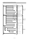
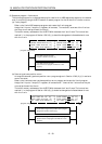
(b) ABS sequence program example
1) Initial setting
To reset the error of the A1SD75, the program 5) is added to reset all output signals at start-up.
The axis error reset buffer memory address is changed from 201 to 1154 (axis 1) and the slot
number from H0001 (slot number 1) to H0000 (slot number 2) 6).
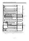
2) Absolute position polarity, A1SD75 rotation direction setting detection
The slot number and buffer memory of the X-axis rotation direction parameter reading area are
changed from [FROMP H0001 K7872 D8 K1] to [FROMP H0000 K5
D8 K1] 8).
The rotation direction parameter masking area is changed from [WAND H0004 D8] to [WAND
H0001 D8] 9).
3) Reversing absolute position polarity
The rotation direction judging area is changed from [= D8 K4] to [= D8 K1] 10).
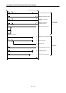
4) Reading checksum 6 bits, reading ABS data 32 bits
The 4 bits reading area is changed from [MOV K1 X30D5] to [MOV K1X20 D5] 11).
5) Restoring absolute position data
The slot number and buffer address of the A1SD75 home position address reading area are
changed from [DFROP H0001 K7912 D9 K1] to [DFROP H0000 K72
D9 K1] 12)