


1
CONTENTS
1. FUNCTIONS AND CONFIGURATION 1- 1 to 1-12
1.1 Summary ........................................................................................................................................... 1- 1
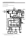
1.2 Function block diagram ..................................................................................................................... 1- 2
1.3 Servo amplifier standard specifications ............................................................................................ 1- 4
1.4 Combinations of servo amplifiers, servo motors, and controllers ..................................................... 1- 5
1.4.1 Combinations of servo amplifiers and servo motors .................................................................. 1- 5
1.4.2 Compatible controller ................................................................................................................. 1- 5
1.5 Function list ....................................................................................................................................... 1- 6
1.6 Model designation ............................................................................................................................. 1- 8
1.7 Structure ........................................................................................................................................... 1- 9
1.7.1 Parts identification ...................................................................................................................... 1- 9
1.8 Configuration including peripheral equipment ................................................................................. 1-11
2. INSTALLATION 2- 1 to 2- 8
2.1 Installation direction and clearances ................................................................................................ 2- 2
2.2 Keep out foreign materials ................................................................................................................ 2- 3
2.3 Encoder cable stress ........................................................................................................................ 2- 4
2.4 SSCNET III cable laying ................................................................................................................... 2- 4
2.5 Inspection items ................................................................................................................................ 2- 6
2.6 Parts having service lives ................................................................................................................. 2- 7
3. SIGNALS AND WIRING 3- 1 to 3-42
3.1 Input power supply circuit ................................................................................................................. 3- 2
3.2 I/O signal connection example ......................................................................................................... 3-11
3.2.1 For sink I/O interface ................................................................................................................. 3-11
3.2.2 For source I/O interface ............................................................................................................ 3-12
3.3 Explanation of power supply system ............................................................................................... 3-13
3.3.1 Signal explanations ................................................................................................................... 3-13
3.3.2 Power-on sequence .................................................................................................................. 3-14
3.3.3 Wiring CNP1 and CNP2 ............................................................................................................ 3-15
3.4 Connectors and pin assignment ...................................................................................................... 3-17
3.5 Signal (device) explanations ............................................................................................................ 3-18
3.5.1 Input device ............................................................................................................................... 3-18
3.5.2 Output device ............................................................................................................................ 3-19
3.5.3 Power supply ............................................................................................................................. 3-20
3.6 Forced stop deceleration function ................................................................................................... 3-21
3.6.1 Forced stop deceleration function ............................................................................................. 3-21
3.6.2 Base circuit shut-off delay time function ................................................................................... 3-22
3.6.3 Vertical axis freefall prevention function ................................................................................... 3-23
3.6.4 Residual risks of the forced stop function (EM2) ...................................................................... 3-23
3.7 Alarm occurrence timing chart ......................................................................................................... 3-24
3.7.1 When you use the forced stop deceleration function ................................................................ 3-24
3.7.2 When you do not use the forced stop deceleration function ..................................................... 3-25
3.7.3 Hot line forced stop function...................................................................................................... 3-26
3.8 Interfaces ......................................................................................................................................... 3-32