


3. SIGNALS AND WIRING
3 - 33
3.8.2 Detailed explanation of interfaces
This section provides the details of the I/O signal interfaces (refer to the I/O division in the table) given in
section 3.5. Refer to this section and make connection with the external device.
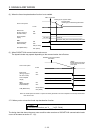
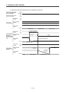
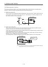
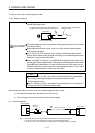
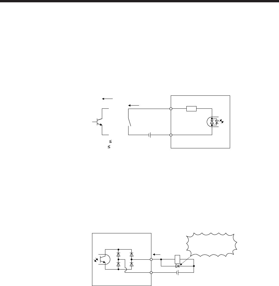
(1) Digital input interface DI-1
This is an input circuit whose photocoupler cathode side is the input terminal. Transmit signals from sink
(open-collector) type transistor output, relay switch, etc. The following is a connection diagram for sink
input. Refer to section 3.8.3 for source input.
Approximately
6.2 kΩ
Approximately
5 mA
V
CES
1.0 V
I
CEO
100 µA
TR
24 V DC ± 10%
100 mA
Switch
For transistor
EM2
Servo amplifier
DICOM
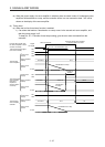
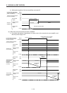
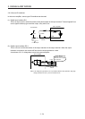
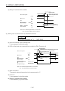
(2) Digital output interface DO-1
This is a circuit in which the collector of the output transistor is the output terminal. When the output
transistor is turned on, the current will flow from the collector terminal.
A lamp, relay, or photocoupler can be driven. Install a diode (D) for an inductive load, or install an inrush
current suppressing resistor (R) for a lamp load.
(Rated current: 40 mA or lower, maximum current: 50 mA or lower, inrush current: 100 mA or lower) A
maximum of 2.6 V voltage drop occurs in the servo amplifier.
The following shows a connection diagram for sink output. Refer to section 3.8.3 for source output.
(Note) 24 V DC ± 10%
100 mA
If polarity of diode is
reversed, servo amplifier
will malfunction.
Servo amplifier
MBR
Load
DOCOM
Note. If the voltage drop (maximum of 2.6 V) interferes with the relay operation, apply high
voltage (maximum of 26.4 V) from an external source.