


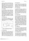
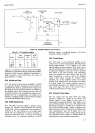

Model
34904
Attenuator
is
switched
by
reed
relays
which are con-
trolled by
signals
from
the
DC Switching
Logic
circuits'
No attenuation
is
used
on
the .l
V, I V and 10 Vdc
Ranges.
Attenuation
of
100
is
used on
the 100 V and
100Ö
V ranges.
No
attenuation
is
required
for resistance
measurements,
because
the full-range
voltage across
the
resistance
being
measured
is
not
greater
than
l0 V. In ac
voltage
measurements,
the AC Converter
output is
applied
to
the
DC
Amplifier
through a FET
(Field
Effect
Transistor)
switch,
and
the dc
attenuator
is not used.
+23.
DC
AmPlifier.
424.
The DC
Amplifier
is
a differential
amplifier
circuit
using
a
FET
input
stage
to
provide
an
input resistance
sreater
than
l0ro
ohms on
the
.l V,
I V
and
lOV
i*g.r.
Input
resistance
on
the 100
V
and 1000 V ranges
is
l0MO,
as
determined
by
the
attenuator.
The
push-
pull output
stage is
protected
by diodes which
prevent
excessive
output
current.
The
amplifier output
is
f
or
-
10 V
full
range
for aU ranges and
functions.
In normal
operation,
this
output
is
applied
to
the Integrator
circuit.
If
optional
Sample/Hold
operation is
selected,
the DC Amplifier
output
is applied to the
Sample/Hold
Analog
circuits.
+25.
OC
Amplifier
Gain.
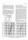
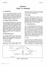
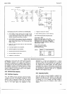
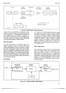
4-26.
T\'rc
gain
of
the DC
Amplifier
may be l,
l0
or
100, and
is determined
by
the
feedback
path
selected.
FET switching circuits are used
to select the fee{back
resistance
ratios, and the
gain
is
equal
to
FRI-I
-FR2,
as
shown
in Figure 4-3.
FR2
OUTPUT
ARI
9.9
M
aMPLTFIEF CA]N
-
--i-
FRI
AR2
O.IM
aTTENUaTToN,
aR2
$
$
GA N
FRI FR2
xr
o
roox
xro 90K
roK
xroo 99K
x
Figure 4-3.
Simplified
Diagram, DC
Amplifier.
Section
IV
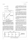
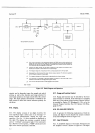
4-29. Boottrap
Circuit.
4-30.
The
gate-to-source
bias for
the
switching FETs
is
provided
by a
voltage
which
is
bootstrapped to the
DC
Amplifier input voltage
to
provide
the
proper
turn-on
and turn-off bias.
The input
of
the
unity-gain
Bootstrap
Amplifrer,
shown
in Figure
7-20,
is connected to the
DC
Amplifier feedback line.
l[.31.
Reference
Voltages.
4-32.
lnternal
reference
voltages are
provided
for
the
run-down
portion
of the
measurement
sequence. In
dc
measurements, if the input voltage is
positive,
the
-
l0
V
reference is used; and
if the
input
is negative, the
+
l0
V
reference is
used.
In
ac measurements,
the
AC Converter
output is positive
requiring
the negative
reference for
run-down. The
Sl
reference, used in resistance measure-
ments,
is
generated
by the Ohms
Converter
and is
approximately
-
I V.
4-33. Overload Protection.
4-34. Protecfion
against excessive input voltage is
pro-
vided at the DC Amplifier input.
On
the 10
V, 100 V
and 1000V
ranges,
the
input is limited by breakdown
diodes to
approximately
1
13
V. On the .1 V and I
V
ranges, the
protection
circuits
are
switched to limit
the
input
to the
amplifier
to
approximately
x
2
V.
Overload
protection
is also
provided
at
the
amplifier output by a
diode circuit in
parallel
with
the
feedback
attenuator.
If,
for
example, the amplifier is operating
with a
gain
of
l0
or 100
and
the
output voltage exceeds
approximately
+
l6 V, the
diode
circuit
begins to conduct,
reducing the
amplifier
gain,
with
a
corresponding
reduction
in
output
voltage. If the
amplifier is operating
with a
gain
of
l0
or
100, the
gate
of the xl
gain
FET
(K
in Figure
44)isar
-
17
Y.If
the amplifier output
goes
excessively negative,
as
it
approaches
-
17 V, the
xl
gain
FET begins to turn
on, reducing the
amplifier
gain
and its output
voltage.
€onsequently, the
amplifier
output
is
limited
to
approxi-
mately
1
16
V.
4-35. Leakage
Gontrol.
4-36. A
FET switch
(B
in Figure
44)
is
also
provided
which disconnects the three
reference FETs
(F,
G,
H),
the
AC
Converter output FET
(E),
and
the
.01 Attenua-
tor FET
(D)
from the
amplifier input
during run-up
when
the
xl
Attenuator line is
being used. This reduces
the posibility
of leakage
from
these
circuits
into
the
high impedance
DC Amplifier input circuit.
4-37. DC Amplifier
Auto Zero.
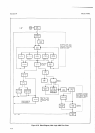
4-38. During
certain
portions
of
the
measurement
se-
quence,
as shown
in
Figure
44,lhe DC Amplifier
circuit
is automatically
zeroed. At the completion
of a measure-
ment, the amplifier input
is
grounded
through
the Input
Short FET switch
C. The
Auto
Zero
signal
then turns
on
FET
switch J, placing
the
amplifier
in a
xl
gain
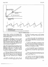
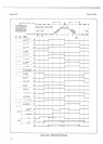
4-27.
Switching
Circuits.
4-28. Figure
4-4
shows
the
3490A measurement
se-
quence.
During
the
charging,
or run-up
period, the input
sigtal
is
applied
to
the
DC
Amplifier
input.
During
the
discharge,
or
run{own
period,
the
proper
reference
is
applied.
Switching
of these
signals
and
others such as a
Feedback
Attenuator
and
Auto
Zero circuits.
is
accom-
plished
by FET
switching
circuits.
These
FETs
are all
contahed
in
one
microcircuit
package,
A2UZ, and are
driven
by signals
from
the
DC
Switching
Logic
circuits.
4-3