


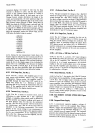
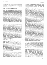
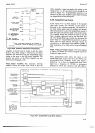

Model3490A
Figure
4-26. Dielectric
Absorption
Compensation.
Amplifier
is shorted,
and its output
is only the
offset
present. This
offset voltage
is
inverted
by the
Offset
Amplifier and
subtracted
from the
Sample/Hold
sigral
voltage
at
the input to the
S/H Output Amplifier.
The
purposg
ald action of
the
Offset Amplifier
are also
mentioned in
Paragraph
4-220.
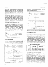
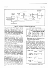
4-227.
Output Amplifier. This unity-gain
inverting
amplifier inverts
the
output from
Circuit
B
(less
the
Section
IV
Offset Amplifier
output)
and applies
this
voltage
to
the
Integrator (A
-
to
-
D
Conversion)
circuit
through
Kl,
as
shown
in Figure
4-31. If
Sample/Hold
operation
is
not
selected,
th9 DC
Input
Amplifier
output
signal
by-passes
the
Sample/Hold
circuits
through
K2.
4-228.
Sample/Hold
Logic Circuits.
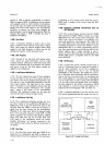
4-229.
Fipre
44,7
is
a block
diagram
of the
Sample/
Hold logic
circuits.
The
function
of
each
block
is
discussed
in the
following
paragraphs.
The
sequence
of
the
main
timing
signals
must
be modified
for
Sample/
Hold
measurements
to
allow the
Sample/Hold circuits
to
track the
input
and
reference
signals
at
the proper
times.
The
modified
timing
also
grounds
the
input
to the
DC
Input
Amplifier
during
the
run-up
and run-down
peri-
ods.
The
Sample/Hold
logic circuits
also determine
the
proper
delay
for
Acquire/Hold
measurements
in
accor-
dance
with the
range selected.
The
logic
circuits
are
controlled
by
an Algorithmic
State Machine
(ASM).
A
brief explanation
of
an
ASM
will
be found
in
paragraph
4-90.
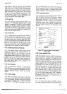
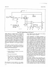
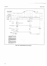
4-290.
Timing
and
Trigger
Circuits. The
block
diagam
in
Figure
4-28
details
the circuits
and
sigrals
used
in
the
timing
and trigger
circuits.
4-231.
Sample/Hold
State
Clock. The input
to
the
Sample/Hold
State
Clock comes
from
the 34904
crvs-
tal-controlled
Clock
Oscillator,
A1U3.
This
signal
is
divided
by 16, so
that
the
Sample/Hold
State
Clock
sigral
has
a frequency
of
250 kHz
in instruments
desigred
for
60 Hz
line
operation,
and
208.3
kHz
in
+4V
HOLO 8
OV
crRcurr B
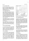
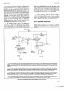
+lov
OUTPUT( ooint
O)
'
-tov
+t8OmV
VOLTAGE ACOSS
R5
(poinr
G)
ev
+l80mv
+l8Omv
oa coMPENsATtoN
^.,
AMPLIFIER OUTPUT
VY
(
Dolnl H)
"
-l8OmV
*
coupeNsaltlc
VOLTAGE ACROsS
CIO
(polnr
F)
*
lye
e outpur
WITHOUT
COTPENSATION
OV
*
TxEsE
wav€FoRMs
EXAGGERATEo
FoR
puRposEs
oF
ILLUSTRATION.
CANNOT
8E
OSSEFr'ED
ON OSCILLOSCOPE
1490-8-3432
SAMPLE/AOLD CL@K
FFOM
g$A
MAIN
CL@K
O$ILLATOR
EXTEiNAL
SMPLE/HOLO
TRIGGEA
INHIAIT
$MPLE/HOLD
FFW
A$II
@TION
TURN.ON
CLEAF
FROM
g9OA
MAIN
LGIC
r*m
r"orr
[
"A^G€
PANET
CONTROLS,
,/
S
F€MOI€
OPTION.
\
ENAALE
oa asl
OpTtoN
I
gH
\MODE
MAIN
TIMING
SIGNALS
{TrME BtTSC,8,A)
FRil
34SA
MAIN
LOGIC
I
I
-
IO
STATE STOAAGE
yr
uooe
)
sELEcrEo
I
Tos/H
HoLo
a
/äl$t?,".
I
NOLD A '
MAIN TIMING
SIGNALS
TO
E
SWITCHING
IOGIC
(SOU€NCE
MODIFIEO
WH€N
Sß
MOOE
SEIECTEDI
S
MOOE
S€LECTEO
TO rcO
OR N[
@Trfr
ßATIO
rcLARITY
NOTE
I
@nEo
LrNES r{Or.
CATE
SIGNAI PAGS
wtcH uusT
BE
Cq.
PL
E TEO FOR
THE
3490A TO
EERATE
WITA
SAIPIEAOLO
iErcV€D
OISLAY POLAFITY
IO
OI$LAY ANO
g9OA
MAIN
LGIC
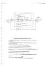
Flgure
4-27.
Sample/Hold
Logic Block Diagram.
+25