


Section
IV
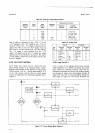
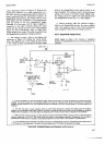
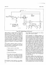
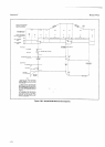
4-223. Circuit
B.
A
simplified
diagram
of
Sample/Hold
Circuit
B
is shown
in Figure
4-25. The
operation
of
Sample/Hold Circuit B is similar
to the
operation
of
Circuit A. Circuit B
responds
more slowly than
A
and
is
able to
hold a constant
output level
long
enough
for
an
accurate measurement
to
be
completed.
To
allow
time
for Circuit B
to respond to the
output
of A, the
B
Hold
command
occurs
about 2 milliseconds
after
the
A Haid
command. The purpose
of the
amplifier
circuit shown
in
Figure 4-25
between
points
D and F
is to
compensate
for
dielectric
absorption
in the integration
capacitor,
cr2.
4-224.
Dielectric
Absorption.
Dielectric
absorption is
the
memory
effect
of a
dielectric
when the
voltage
across
the
capacitor is
changed
suddenly.
This
may
be
illustrated
by
the following
example:
l.
Charge
a
capacitor
to
a
given
voltage.
2.
Quickly
discharge the
capacitor to
zero
with
a
small
load
resistance.
3.
Disconnect
the load
resistor.
4.
The
voltage
across the
capacitor
will increase
slowly
from
zero in the
direction
of the
voltage
applied
in
step
l. This voltage
will develop
quite
slowly,
but
could contribute
several
counts
of
error
in the
Sample/Hold
measure-
ment.
This
phenomenon
becomes
significant
in
the
Sample/
Hold inreerator
circuit
when
the
voltage
applied to
this
I
rl
Model3490A
circuit
changes from the input
signal to
the
reference
voltage, which is
opposite in
polarity.
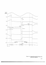
4-225. Compensation
for
Dielectric Absorption.
To
prevent
deterioration
of the
Sarnple/Hold
output
signal
due to
dielectric absorption,
an amplifier circuit
is
used
between the
output
of Circuit B
and
the
non-inverting
input to the
integrator portion
of
this
circuit
(pqints
D
and F in Figure
4-25). The
waveforms in
Figwe
4-26
help to
illustrate the
action
of the Dielectric
Absorption
(DA)
Compensation circuit.
During
the
Track
Mode,
55
and
36
(Figure
4-25)
are closed.
Any
change in
the
output
voltage at
point
D causes current
to
flow through
the rc
circuit R34, Cl6
and R6. This
current
decreases
as
Cl6
assumes the new
voltage. The
resulting
voltage
across
R6 is
applied
to
Cll
and
the
DA
Compensation
amplifier
input.
When
a Hold B
command
occurs,
55
opens
and the voltage
across
Cl
I
remains
at
the
level
present
at
that
moment.
56 also
opens
at
this
time,
allowing Cl8 to begin
charging
slowly
toward
a voltage
proportional
to
the
charge
on C11. The
compensating
voltage
at
point F is the
voltage
developed
across
Cl8.
As
the
time increases between
a
voltage change
at the
integrating capacitor and the
Hold
B command,
the
need
for
compensation decreases,
and the
compensation
provided
also decreases.
4-226.
Ottset
Amplifier. During
Sample/Hold opera-
tion,
the Auto Zero
circuit
for the DC Input
Amplifier is
disabled; consequently, some
offset
voltage may
be
present
in
the amplifier
output. This offset
will
be
included in
the
voltage held
by Sample/Hold
Amplifien
A
and
B.
During
both the
run-up
and run-down
portions
of the
measurement
period,
the input to the
DC
Input
+I7V+I7V
INTEGRATING
OUTPUT
OF
S/H
CIRCUII
(D
R8
-
20K
@
OUTPUT
R58
7tK
R39
7r K
R34
tooK
S4,S5, AND
55 ARE
FET
SWITCHES.
THEY
ARE ALL
OFF
(NOT
CONDUCTING) FOR
THE
HOLD MODE.
D A
COMPENSATION
-t7v
@
S5
ct6
o.47
v
t8
R36
roo
R6
toK
J490
A-B-3433
Ja+z
v
Figure 4-25.
Simplified Diagram
of
S/H
Circuit
B.