


Model3490A
tl-90.
Algorithmic
State
Machine.
4-91.
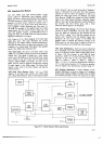
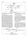
T\e
3490A
main
logic
circuits
employ a
logic
svstem
called
an
Algorithmic
State
Machine
(ASM)'
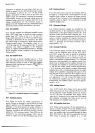
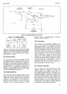
Fizure
4-9
shows
a
typical
State
Machine
block diagram'
nir
nSU
outputs
are
determined
by
the
"state"
of the
machine
at
a
given
instant,
called
the
"present
state'"
Certain
outputs
in
the
present
state, along
with
one or
more
"qualifier"
inputs,
determine
the
"next
state" of
the ASIr{.
For
example,
if the
qualifier
input is a certain
timing
signal,
the
Next
State
Function
logic may wait
until
this
qualifier
reaches
a
predetermined
level to
change
the
state
of
the
ASM.
Each new
state
provides
a
different
combination
of
outputs.
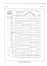
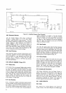
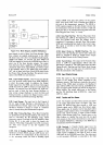
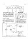
492.
Figore
4-10
is
a
block
diagram
of
the
main
logic
ASM
flow
chart.
This
chart
illustrates
the
process
followed
by
the
ASM
in
taking
a normal
measurement'
Note
that
at
many
points,
the
path taken depends
on
the
condition
of a
certain
signal.
This
signal
is the
qualifier
input
to
the
ASM at
that
particular
time.
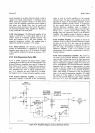
4-93. State
Clock.
The input to the State Clock
is
the
4MlIz
(or
3.333 MHz) output
from the
Clock Oscillator
(Figure 4-8).
This
signal
is
divided by a
4-bit
binary
counter
and a
D flip-flop, so
that the
State Clock
output
has a
period of
8
prs
(or
9.6
ps).
The
two
State Clock
outputs,
labeled
HSCK and
LSCK, are
180"
out of
phase, and are used for alternate
synchronous clocking
of input
signals to the ASM storage. The State Clock
output
is
also
used
in the Data Output and Remote
Control
circuits.
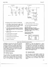
4-94. Read Only
Memory.
Figure
+11
is a block
diagram
of
the
Main
Ingic Circuits.
The 3490A
logic
uses a
Read Only Memory. Seven
of
the memory
inputs
Section
IV
in
the
"present"
state
are used, along
with
a
"Qualifier',
input,
to determine the
next state. Five
other
memory
outputs are used
to select
the
qualifier,
as
well
as
to
initiate the
other logic
action.
In
addition, the
Read
Only
Memory
(ROM)
also
supplies
an
Output Enable
sipal to the
Logic
Output Decoder,
a
Memory
Output
sigrral
to
the
Logic
Storage flip-flops, Transfer
Enable
to
the
Transfer
utd Zero
Detect
gates,
and
a
Close
Electronic
Switch signal to
the
Integrator.
4-95.
Present
State
Storage.
The Present
State
Storage
consists
of seven
D flip-flops.
The next state
outputs
from the
ROM
are
clocked
into the flip-flops
by the
State
Clock
L signal. The
D flip-flop
outputs
are the
present
state.
Together
with the
qualifier
input,
they
determine
the next
state outputs
of the
ROM. The
qualifier
input
is
clocked into
memory storage
at
the
ROM
input by
the
State
Clock
H signal
4
ps
later
to
prevent
uncertainty
in the ROM next state
decision.
4-96.
State
ldentification.
Each state
may
be identified
by a three-digit
octal coded
number
determined
by the
levels
of
D flip-flop
outputs YMA
through
YMG, shown
in Figure
7-30. For
example,
in state
000,
all seven
outputs
are LOW
("0").
If
only
YMA goes
HIGH
("1"),
the
state
is
then
001.
In the
state
where YMG=
l;
YMF=0;
YME=l;
YMD=1;
YMC=l;
YMB=l;
YMA
=
I
(l
0l
1
I l1), the
state identihcation
number
is
131
.
A total
decimal number
of 128
states
are
possible,
with the
highest
state
identification
number
being
177-
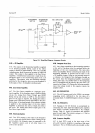
4-97.
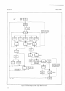
Oualifier
Multiplexer.
A
block diagram
of the
Qualifier
Multiplexer
is shown
in Figure
4-1
2.
Qualifier
Enable
signals
LMQA,
LMQS,
and
LMQC from the
ROM
are
inverted
and used
to select
one output
out
of eight
Figure
4-1
1.
Block Diagram, Main
Logic Circuits.
4-l
r