


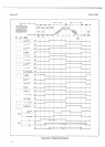
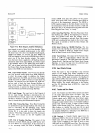

Section IV
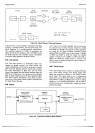
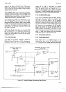
ENAELE
I
NPUTS
OUALIFIER
INPUT
TO ROM
ENABLE
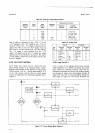
Figure
4-12. Block
Diagram, Qualifier Multiplexer.
input
signals
to each of three 3-to-8
line
decoders.
These
three outputs
are applied simultaneously to
the AND/
OR Invert
Gate. The other two
Qualifier
Enable sigrals,
I-il,IQD
and LMQE, are inverted
and both
HIGH
and
LOW
true signals
are
used
at
the
AND/OR
Invert
Gate
to
select
one
of
the three
decoder outputs. The output
from
the Invert Gate is
applied
to a D flip-flop, which
is
clocked by State Clock
signal HSCK,
and
whose
output
is
the
Qualifier
Input to the ROM. This clock
signal is
180" out of
phase
with
State Clock LSCKwhich
clocks
the Present State
Storage
flip-flops. This
prevents
uncer-
tainty in the ROM next state
decision.
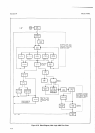
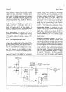
4-98. Logic Output
Decoder.
This
4-to-l6line decoder
uses
four inverted
enable signals
from ROM, HMQA-D,
to
select the
proper
output. In
addition, the Output
Enable signal
from the
ROM, and
the
State
Clock signal
LSCK
must
both
be LOW
to
obtain
an
output from the."
decoder. All outputs
from
this
decoder are
LOW
true,
and
are used to
clock the
Logic
Storage
flip-flops,
to
clear certain
storage flip-flops,
to clear
the
Data and
Timing
Counters, to operate the
Range Counter, and
to
clock the'Polarity
and Overload storage flip-flops.
4-99.
Logic
Storage.
The input
level to
the
D
inputs
of
the six
Logic
Storage flip-flops
is
determined by
the
inverted Memory
Output signal from
the
ROM.
Each
flip-flop
is clocked
to
change its output at
a
different
time
(or
times)
during
the measurement sequence.
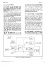
4-100.
Main
Timing
Flip-Flops.
Three Main
Timing
Bits
are
produced
by
Logic
Storage
flip-flops. All of
these
are
used
in controlling
the
DC
Switching
Logic, which
determines inputs
to
and
gain
of the
DC Amplifier.
Main
Timing Bit
A
is
also
used
to
drive
the
sample
rate
indicator. When
Main
Timing
Bit B
is
LOW,
it
activates
the
Auto
Zero
circuits
in
the
DC Amplifier and
Integrator.
tl-101.
End
of
Reading
Flip-Flop. The output of
this
tlip-t1op
is
normally
HIGH,
and
goes
LOW
shortly
after
the Zero Detect
of
a measurement.
If the instrument is
Ln
the
autorange
mode, the
End of Reading
sigral
Model
3490A
remains
HIGH until after
Zerc Detect
on the
correct
range. After
going
LOW,
End of Reading
goes
HIGH at
the
end of
the
measurement
sequence.
The
HIGH
to
LOW
transition
signals
to the
Data Output
circuits that
the information
stored
in the
Data Counter
is
valid
and
allows
the
data
to be
transferred across
guard
before the
Data
Flag
goes
from
"busy'
to
"ready."
4-1O2. Data Flag
Flip-Flop.
The Data
Flag output from
this flip-flop
goes
LOW
at
the beginning of a measure-
ment and remains LOW
until
the reading
cycle
is
completed.
If
autorange
is selected, Data
Flag
remains
LOW
until a reading
has been
made on the
correct range.
This
signal is
inverted in both
the Data Output and
Remote circuits.
4-103.
Select
Divide by
100,000
Flip-Flop.
The two
outputs
from this flip-flop are
used to
select
either
the
divide
by
100,000 or
divide
by
10,000 counts
output
from
the
Data Counter
to the Timing Counter.
4-104. Turn-On
Clear.
The output of
the
Turn-On Clear
circuit is
LOW
for approximately
100
ms after
the
instrument is tumed on. This LOW
signal clears the Main
Timing
B
and C
flipflops and
the Present
State Storage
flip-flops, to force
the logic into the
preferred
state
when
the instrument is first
turned
on.
4-105.
Input Polarity
Storage.
4-106.
The
input to this D flip-flop
is the
inverted
output of the Analog
Zero Detect Amplifier
in the
lntegrator
circuits.
The flip-flop
is clocked at the end of
run-up.
If the 34904 input is
positive,
the flip-flop D
input will be LOW at
the end of run-up, and
HIGH if
the
input
is
negative. Both outputs are used
in
the logic Zero
Detect circuits.
The
output
which
goes
to the
Display
and
the
DC
Switching
LoSc
is
HIGH for
+
input
and
LOW for
-
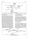
input.
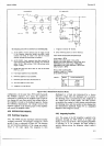
4-107. Transfer and
Zero
Detect.
4108. The
Transfer
and
Zerc
Detect
circuits are
shown
in the
upper
right
hand
corner
of
Figure 7-30. Two
outputs
are derived
from
these circuits;
a
LOW
true
Transfer
signal,
and
a
HIGH
trve Zerc
Detect sigtal.
These signals
may
be
issued at
end of run-down
(when
Integrator
output
reaches
zerc), at overload
if reading
is
greater than
120
%
of nnge,
or when
a
False
Transfer
signal
is
given during
Logic
Test. Transfer
goes
to
the
Data
Counter
to
transfer the count
into
the
six
quad
latch
circuits
in
the
countet.Zero
Detect
is one
input to
the
Qualifier
Multiplexer,
indicating
to the ROM
that a
measurement
has
been
comPleted.
4-109. Overload.
A Transfer
Enable signal from
the
ROM
goes
HIGH
at
the
start of run-down,
and
remains
HIGH until
after
the Transfer sigral
goes
LOW.
This
enable
signal
is applied
to
one
input of
each of
three
AND
gates
in
the AND/OR
Invert Gate.
The other
input
to the
two-input
AND
gate
is connected
to the Time