


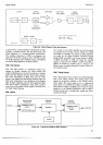
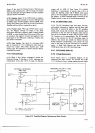

Model3490A
Count
32 line
from
the
Timing Counter.
This line goes
HIGH at
the overload
point,
120
7o
of runge. The
output
from
this AND
gate
then
goes HIGH to
produce
Transfer
and
Zero
Detect
commands.
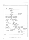
4-110. Negative
Input.
If the
34904
input is
negative,
the
Polarity Storage
Q
output
to
the next AND
gate
will
be HIGH.
Since
Transfer
Enable is
already HIGH,
when
Analog
Zerc
Detecr
goes
HIGH at
the
end of run-down,
Transfer
andZero
Detect
commands
are
given.
+111.
Positive
Input.
When Jhe 3490A
input is
posi-
tive, the
Polarity
Storage
Q
output
to
the
other
three-input
AND
gate
is
positive.
Again, Transfer
Enable
is HIGH,
so when
Analog
Zero
Detect
goes
LOW at end
of rundown,
this signal is inverted
and applied
to the
third input
of
the AND
gate,
resulting
in
Transfer
and
ZercDetect
commands.
4-112. False
Transfer. One
input
of
a
two-input
AND
gate
is
connected to
f
5
V, enabling the
other input to
control
the output. When False Transfer goes
LOW
during Logic
Test operation, Transfer
and Zero Detect
commands
are
issued.
4113.
Ovedoad
Storage.
+114. When
a Zero Detect command
is issued,
the
Overload
Storage D flipflop is
LOW, indicating
the
measurement
is less than l2OVo
of
range,
the
flip-flop
Section
IV
output
will
be LOW.
If
Time
Count 32
is
HIGH,
indicating
a measurement of
greater
thm
120
% of
range,
the
flip-flop
output
will
be
HIGH.
T[ris
output
goes
to
the Data
Output circuits
(Option
021),
and to
the
Display. A
HIGH
Overload
sigral is
inverted
in
the
Display
circuits to turn
on
the
Overload annunciator.
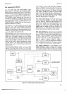
+il5.
DC
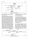
SWTTCH|NG LoGrC.
4-1 16. The
DC
Switching Logc uses
range, function,
and
polarity
information, together
with the
three
main
Time Bits to
control
all
inputs
to the
DC
Amplifier
during both run-up
and run-down. This
includes
input
protection
on the
two
lower
dc Ranges, input
attenua-
tion
on the two
higher
dc
ranges,
and the
output
ofthe
AC
Converter
in
ac
measurements.
The
DC
Amplifier
gain
is also selected
by the DC
Switching
Logic. In
addition,
this circuit
also enables
the
Ohms
Converter
during
resistance
measurements,
and
controls
the
reed
relay
at the input to
the AC
Converter
for ac measure-
ments.
A
,Read
Only Memory
and three
dual-input
NAND gates
make up
the DC
Switching
Logic.
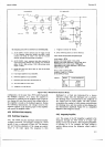
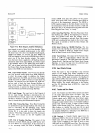
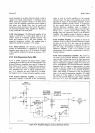
+II7. REFERENCE
SUPPLIES.
ll.l
18.
Voltage Mea$rements.
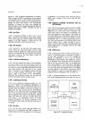
4-119.
Figure 4-13 is
a
simplified
diagram
of the
Reference
and Ratio circuits.
An
accurate
and stable
+
l0 V
Reference from
a voltage
regulated
power
supply
EXTERNAL REFERENCE
AMPLIFIER
(oPTloN
o80)
REFERENCE
POLARITY
LOGIC
(oPTtoN
080)
INPUT
POLARITY
EXT REF
INPUT
RATIO POLARITY
EXT
INT
+REFERENCE
SUPPLY
aLL
JUMPERS
_<*-b_ REMovEo
tF
RATIO
OPTION
IS
INSTALLEO. I
,rtl
+REF
sENsE I
3490-8-2930
Figure
z1-13.
Simplified
Diagram,
Reference
and Ratio
Circuits.
+13