


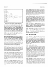

Section IV
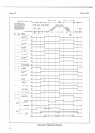
466.
0hmmeter
Reference.
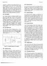
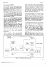
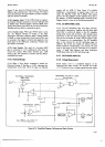
Figure
4-7.
Simplified
Model 3490A
Diagram,
Ohms
Converter.
proper
combination
of signals
to
the
Scan
Decoder.
Three
scan
signals,
A,
B,
and
C, are applied
to the
Data
Counter
to release
the stored
BCD
count
information
one
digit
at a time,
beginning
with the
least
significant
digit, Nl. These
scan
signals
are
also used in
the
Data
Output
and Remote
circuits.
4-75.
Scan Decoder.
4-16. The
four signal
outputs
from the
Scan Generator
are
fed into
a 4-to-10
line
decoder. The
decoder
then
applies
an enable
pulse
to
each
display unit
at the same
time
that
unit
receives
the BCD
count
information
from
the
Data
Counter.
Scanning is
continuous,
with
all six
display
units
being
scanned
in
approximately
1.6
ms,
beginning
with the
least significant
digit,
Nl.
4-78.
The
function
signals,
from either
the
front panel
switch
or remote control,
are
gated
so
that the
symbol
is
disabled
during
ac and
ohms
measurements.
When
the
symbol
is enabled,
the minus sign
is
on continuously,
and the
vertical
bar is
turned
on when the
reading
is
positive.
The sample
rate
indicator,
contained
in the
polarity
unit, is on
when Main Timing
Bit
A
is HIGH.
4-79.
Decimals
and
Annunciators.
4{0.
Range information
from
the
Range
Counter
is
gated
to turn
on
the
correct
decimal
for each
range.
The
Overload
annunciator is
turned
on by the
Overload
signal
stored
in the
Logic. The
Remote
annunciator
is
driven
by a
circuit
on the
Remote
Assembly.
The
other
annunciators (optional)
are turned
on
by
gating
the
Function
signals. Each
annunciator
is
a single
LED.
4.81.
L0GrC
C|RCU|TS.
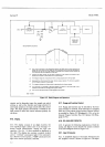
4-82.
Clock.
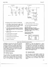
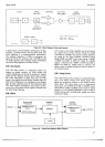
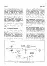
4-83. Figure
4-8 is
a block
diagram
of the
Clock and
Counter
circuits.
The
basic timing
for
the 3490A
Ilgic
+67
. An emitter
follower,
whose
base is
referenced
through
a voltage
divider to
a 5.6
V
zener
diode.
provides
a stable
reference
of
approximately
-
I
V
across
the
reference
resistor
Rrs6
(Figure
4-7).
This
reference
voltage,
applied
to
Rpsg,
determines
the
amount
of
current
supplied
to
R1 by
the
current
source,
as
explained
in
Paragraph
442. A
resistance
measuremenr,
then,
is the
ratio
of the
voltage
across
R* to
the
voltage
across
R1s;,
both
voltages
being
determined
by the
current
resulting
from
the
reference
voltage.
468. Input
Protection.
4-69.
Protection
against
excessive
voltage
which
may
be
accidentally
applied
to
the front panel
Q
Signal
termi-
nals
is provided
by
a
gas
discharge
device
across th:ä
terminals
and
a resistance
in series
with the
hieh
terminal.
Voltages
in
excess of
250 Vrms
may
deströy
the I
kfl
series
resistor.
+70.
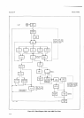
0ISPLAY
ASSEMBLY
(Figure
7-2?).
471.
Display
Units.
4-72.
Each
of
the
six
numerical
display units
contains
a
4
x
7 dot
matrix
of
light-emitting
diodes
(LED$
to
form
the
digits.
In
addition,
each
unit
contains
a decoding
circuit
to
light
the proper
LEDs,
and
a latching
circuit,
so
that the
display
can
be changed
only
during
an enable
signal.
Each
unit
also
contains
a
decimal point
to
the left
of the
number.
The polarity
unit
also contains
the
sample
rate
indicator.
Each
annunciator
at
the right
side
of the
display
is
a single
LED.
473.
Scan
Generator.
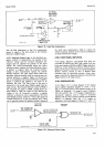
+74.
A relaxation
oscillator
operating
at
approximately
l0 kHz provides
the
clock
signal
for
the
Scan
Generator.
The
oscillator
output
drives
a 4-bit
synchronous
counter.
The
counter
outputs
are
gated
and
fed back
to
reset the
counter
after
every
I
2th input
cycle, thus
providing
the
-1-ö
FEE D BACK
OURING
RUN.DOWN
ONLY
I
,oo.
/
rnre
)
'J
K1
I
I
V
O
REF TO
DC AMP
CURRENT
RRer
1APPROX l
,I
K I K
1K IK
10 K I K
100 K
100 K
1.000 K
100
K
10.000 K
1 lvl
l0
!A
l0
!A
CURBENT
SOURCE
6.8K