


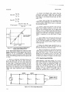
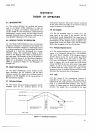
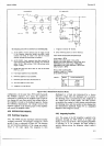

DC
AMPLIFIER
ac
coNv
OUTPUT
J6N'AUTOZERO
I.AUTO ZERO DISA6L€,
USED ONLY DURING
SAMPL€/ HOLD
OPERAIION
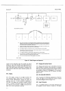
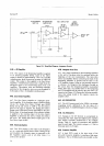
The
following notes refer to waveforms
on
preceding
page:
A.
AUTO
ZERO: lf
hold is
selected, wait
for
trigger. lf hold
is
not
selected,
determine sample rate
delay. Check
function
and
range. lf range is
not
valid
for function
selected,
uprange
and downrange as
necessary.
8.
AUTO
ZERO:
Insert
response
time delay
required for
range and
function
selected. DC
=
0
delay; AC
=
85
ohms
delay; 10
Mo
=
350
ms
delay; 1
MA
=
50
ms
delay; other
ranges
=
0
delay.
C.
Range
gain
with
input
short
(FET
Cl.
Gain can
be
either
FET K,
L, or M.
D. Input signal
applied
to input
amplifier.
E.
Reference applied
to
input
amplif ier.
F.
Reference
gein
with input
shorted
(FET
K).
G. Auto
Zero
(65
ms of
auto
zero).
H. Integrator run-rup
(50
ms).
NOTE 1.
J. Integrator rundown
(0
-
60 ms).
K.
Select
reference
polarity
or
ohm's
reference.
HIGH TRUE WAVEFORM
INFORMATION
AUTO ZERO
=MT-B
SIGNAL
VOLTAGE
GAIN
=
MTA, MTB
SIGNAL
VOLTAGE APPLIED
=
MTA. MTB, MTC
REFERENCE
VOLTAGE GAIN
=MTA,
MTB
REFERENCE VOLTAGE
APPLIED
=
ili=iÄ, TUTC
INPUT SHORT
=
MTC-
MTA,
B AND C ARE SAME
AS
MDA,
B AND C IF THERE
IS
NO
SAMPLE/HOLD.
MODE
PULSE
INTERVAL
DC
AC
ol M
s,10 M
65
ms
915
ms
115
ms
415 ms
Figure
4-4(b). Measuibment
Sequence Notes.
Model
34904
configuration.
At
the same time,
FET
switch
N
grounds
the
feedback
capacitor.
As
a result, the capacitor is
referenced
to
ground
and
the
amplifier input is held at
zero
during the
Auto
Zero
period.
Any residual offset
in
the
amplifier
is
stored
in
the feedback capacitor. During
the
following
measurement,
the voltage stored in the
capacitor
appears
at
the
inverting
input of the amplifier
and cancels
the
amplifier
offset.
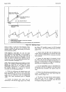
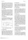
4.39.
INTEGRATOR
CIRCUITS.
440. Dual-Slope
Integration.
4-41. The 34904
uses the
dual,slope
method
of analog-
todigital
conversion.
The
integrator
charges
for a fixed
period
of time,
as indicated
in Figure
44.
The charging
rate and resulting
amplitude
of the
charge are
propor-
tional to the
input
signal.
The
integrator
is
then
discharged
at a fixed
rate
determined by
a known
reference
voltage.
Since the discharge
rate
is
constant,
the
discharge time
is
proportional
to the
amplitude of
the
charge
(and
the input
signal). The
Data
Counter
accumulates
the number
of clock pulses
received
during
the
discharge time,
and this
number is then
displayed
as
the measurement
amplitude. Figure
4-5 is
a
simplilied
diagram
of
the
Integrator
circuits.
442.
Integrating
Amplifier.
443. Tl're output of the DC Amplifier is applied
to the
Integrator through
the
FET
switch
at
its input only
during
run-up and run-down.
The
Integating
Amplifier
is inverting, so if, for example, the input voltage
is
positive
during run-up,
the integrator
output
ramp
is
negative.
Section
IV
4-5