


Section IV
4-152.
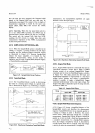
lsolated
Trigger
and
Hold.
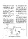
4-153.
External
Encode
and
Hold
are both LOW
true
signals.
They
are
inverted
and applied
through emitter
followers
to
photo-isolators,
consisting of a
light-
emitting diode
which
drives
a
photosensitive
transistor.
Consequently,
there is no
electrical connection between
outguard
and
inguard
circuits.
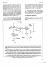
It-l54.
Sample/Hold
Trigger Circuits.
4-155. Sample/Hold
Trigger.
When this
input
goes
from
HIGH
to LOW for a
pulse
width
of at
least 30
nanoseconds,
it signals
the
Sample/Hold
circuits
(Option
040)
to
"hold".
This
pulse is inverted twice and applied
to
an
isolation transformer, which couples
the trigger
sigral
to
the inguard
Sample/Hold
circuits.
The Sample/
Hold Trigger input
connection is direct
coupled,
and if
the
connection
(rear
panel
J7
pin
9)
is
left
open,
+
5 V
is
present
at
that
pin.
This trigger
will
not initiate a reading
unless
the
Stretched
Pulse
Output
is connected exter-
nally to External Encode.
4-156.
AC
Trigger.
This input may
be
any
pulse
having
a
negative-going leading
edge of 2
to 15 volts
and a
width of at
least 30
nanoseconds.
This
pulse is
capaci-
tively coupled to
the
isolation
transformer to trigger the
Sample/Hold
circuits.
zt-157.
Stretched
Pulse
Out.
This output
changes from
HIGH
to
LOW for at
least 240 microseconds
for each
Sample/Hold
or AC Trigger
input.
Stretched
Pulse
Out
may be
connected to External
Encode to
initiate
a
measurement
simultaneously with
the
Sample/Hold
trig-
ger.
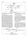
+158.
DATA
OUTPUT
OPTION
021.
4-159.
The Data
Output
connections at the rear
panel
are
isolated
from the internal
circuits of the 3490^.
Power for
the
outguard circuits
is
supplied
by
the
outguard
+
5 V
power
supply. Outguard
ground
is
isolated from inguard
circuit common and
chassis
(earth)
ground,
and may be floated
up to
40
V
above
chassis.
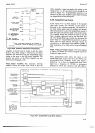
Figure 7-32 is
a diagram of
the Data
Output
circuits.
4-160. Data
Multiplexers.
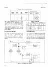
4-161 . Three
multiplexers, each having 8
input lines
and
4
output lines,
are used to transfer
the
Data Output
information
across
the
guard
to
four eight-bit
shift
registers.
An
"output
select"
(Ss)
connection to each
multiplexer
selects
one set of four
inputs if the
Ss
input
is HIGH.
and
the
other set of four inputs
if
Se
is
LOW.
The
outputs
from two
multiplexers are applied
to the
inputs
of the
third,
or
"master"
multiplexer.
The
outputs of
the
master
multiplexer are
enabled for only
the
eights periods
of time
necessary
to transfer
all
the
Data
Output information,
as
shown
in
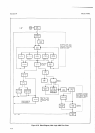
Figure 4-1 8. The
Sequential Logic
determines
the time
and
sequence
of
mlolTnation
transfer.
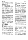
:-l
!
SEOUENTIAL
LOGIC
INPUTS
ENO OF REAOING L
SCAN
C H
SCAN
8 H
I
MASTER MULTIPLEXER
I
I
OUTPUT SELECT
O
I
IIULTIPL€XER OUTPUT
I
ENAELE L
I
I
SCAN
A
H
DATA
MULTIPLEXE
OUTPUTS
OATA
CLOCK
IO OUTGUARO
SHIFT
REGISTERS
ltllllt
rnnnnnnnn
I
o,,oo,o outou,
i.lormorion
tcl.r.d
I
I
oc.cr
ry'd
ddihq
rhi.
e.riod
d iß
i
lltlttlltr
courPursl
I i
I
i
i
I
I
lL--1t..
I lEXr-19
| | dild I
F
i i 16i9'i
3
i"r i98äiä;i
i
lll
lll
rrirztn:lla
Figure 4-18.
Data Output
Timing
Diagram
(Option
021
).
4-162.
Data
Output Sequential
Logic.
zt-163.
Figure 4-18 shows
the timing
sequence of
the
sequential Logic
inputs
and
outputs.
The
Logic
is
enabled when
the End of Reading
signal
goes
LOW
at
the completion of a measurement.
The
three scan
signals
which control
the outputs from
the Data Counter
operate
the
Logic
to correlate
the
multiplexer
outputs
with
the
outputs
from
the
Data Counter.
The
Sequential
Logic
consists
basically
of three
JK flipflops.
The
scan
signal
inputs to
the flip-flops are
gated
to obtain the
desired
output
pattem.
4164.
Oata Clock.
+165.
A
Frequency
Doubler
is used
so that a clock
pulse
is issued for
each
transition
of the
Scan
A signal.
These
pulses
are
delayed
slightly
before
being applied
to
the outguard Shift
Registers,
to
allow
time for the
multiplexer
outputs
to reach
the
proper state.
4166.
lsolation
Asembly.
arl67.
Each
signal
is
transferred across
guard through
a
photoisolator,
which
consists of a
light+mitting
diode
driving
a
photosensitive
transistor.
Consequently,
no
electrical
connection
is
made between
the inguard and
outguard
circuits.
+168. Shift
Registers.
4-169.
Four
8-bit
Shift
Registers are
used,
providing the
capability
of
32
parallel output lines. Each
time a
Data
Clock
pulse is received,
the information
in
the
shift
register shifts
one
position
and a
new input
is
accepted.
A dual-input
Exclusive
OR
gate
in each of
the
shift
register
input
lines determines whether
the coded
Data
Output
information
is HIGH
true
or LOW
true. The
operation
of
these
gates
is such that
if
one
and only
one
input is
HIGH
the output is HIGH.
If
both
inputs are
Model 34904