


Section
IV
Model
3490A
ELECTRONIC
INTEGRATING
SWITCH
AMPLIFIER
XzO AMPLIFIER
ZERO
DETECT
AMPLIFIER
INPUT
FROM
OC
AMP
ANALOG
DETECT
LOG
IC
ZERO
TO
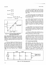
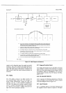
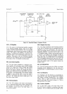
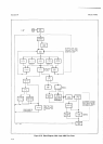
Figure 4-5.
Simplified
Diagram, Integrator
Circuits.
L44. x
20
Amplifier.
445. The
output
of
the Integrating
Amplifier
is applied
to
an inverting
amplifier
having
a
gain
of
20,
whose
output
is limited
to
approximately t
0.6 V
by
a
parallel
complementary
diode connection
between its
input
and
output. This
output is then
applied to
the Zerc
Detect
Amplifier.
A
feed-forward
connection is
made
from the
Integrator
input to the
non-inverting
input
of the x
20
Atnplifier.
This
reduces
noise
and
switching
transieq{s
generated
at the integrator,
since
any noise is
applied to
both inputs
of the x
20 Amplifier
simultaneously.
n
446. Zerc
Detect Amplifier.
447
. The Zero
Detect Amplifier
is a
high-gain
opera-
tional amplifier.
If
the
Integrator
input is positive
during
run-up, the
Analog
Zero Detect
Output
goes
HIGH
during run-up
and returns to
LOW at the
Zero
Detect
point.
If
the
input
is negative, the
Analog
Zero
DeLect
Output
goes
LOW
during run-up
and HIGH
at the Zero
Detect
point.
A frxed
percentage
of the
reference
voltage
is
applied
to
the inverting
input of the
Zero
Detect
Amplifier
to
determine the
level
at which
Zero Detect
will occur.
The
Analog
ZeroDetect
output
goes
to the
Zero
Detect
logic
circuits.
448. Electronic
Switch.
4-49. Two
FET
switches
at
the
input to
the Integrator
act as a sinele-pole
double-throw
switch.
During
run-up
and
rundown.
the
Integrator
input
is
connected
to
the
DC
.tmplit-rer
output,
and
at all other times
it
is
coflreu-tcd to
ground.
J-tt
450.
Integrator
Auto Zero.
4-51. Any charge
remaining on the integating
capacitor
at
the end of rundown
must
be removed
before the
beginning
of the next measurement.
The Auto
Zero
Circuit
accomplishes
this
by
connecting
one input
of the
Integrating
Amplifier to
ground
and
the
other to the
x
20
Amplifier
output. Using its
own inverted
output
as
a reference, the Integator then
discharges through
an
RC circuit.
Since
the Integrating
Amplifier
is
gounded
during Auto Zero,
wry residual offset in the
Integrating
and
x 20
Amplifiers
will be stored in
the Auto
Zero
2
pF
capacitor
(see
Figure 4-5).
During
the following
measure-
ment, this.voltage stored in
the
capacitor
cancels
the
amplifier
offset.
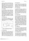
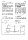
4.52. AC CONVEBTEB.
z1-53.
The
AC Converter used
in
the 3490A
is an average
responding
circuit,
calibrated
to the
rms value
of a
sinusoidal input.
A simplified diagram
is shown
in
Figure
4-6.
4-54. AC Attenuators.
4-55. Ranging
in
the
AC
function
is
accomplished
by
attenuating the
input sigral
and
adjusting
the
amplifier
gain,
which
is
inversely proportional
to the
feedback
voltage.
Table
4-1 shows the
attenuator
and
amplifier
gains
for
each
range. The converter
output is
+
I Vdc
for
full-range
input on all
ranges.
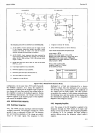
4-56. Converter
Amplifier.
4-57.
A dual
FET is used
in the
input
stage
of the
AC-to-DC Converter Amplifier
to
maintain
a high input
impedance. Two
ac feedback paths
are
provided,
so that