


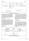

Model3490A
numerical
display;
the length
of time
that the
Data
Counter
is allowed
to
count, and
the Data
Counter
output
to the
Timing
Counter
(divide
by 10,000
or
divide by
100,000
counts).
In each
range,
one
of six
Timing Counter
outputs determines the length
of the
count, and
consequently,
the
most significant
digit. The
position of
the most
significant
digit is
the
result of the
Data
Counter
output
selected. If
Main Timing
Bit
B is
HIGH,
the divide
by
100,000
output is
selected,
and if B
is
LOW, the divide
by 10,000
output is
used. If
Main
Timing
Bit C
is
HIGH,
the
instrument
upranges,
and if
C
is
LOW,
it
downranges.
Both
timing
bits
are set
HIGH
when the
instrument reaches the
lowest
range,
and set
LOW when
the highest range
is reached.
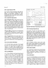
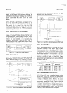
+
080.024
+
O4.0024
+
o.2N24
+.010024
+
0.09032
+
t0.oo24
+
200.024
+
4000.24
+
80002.4
+
6000.xx
OL
4-136.
During
the last
measurement listed
above,
the
Transfer
signal is switched
on for
8 counts and
off for 8
counts
during
the entire
counting
period,
which
lasts
for
1,600,000
+
counts.
Because
of
the
counting
frequency,
nearly
all dots
in the
display
appear to be on
during
this
period.
The I
(in
1,600,000)
is lost
because the display
does
not provide
a
seventh
digit.
In
all except the last
reading, the two
least
significant
digits
are
predictable
because
of known
transition
times during the
reading.
+137.
10
V Range
Zero,Test
No.
2.
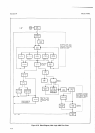
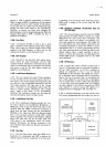
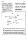
4.138.
Test
No.
2 selects
a DC
Amplifier
gain
of
I
for
both
run-up
and
run-down,
which is
the l0
V range
configuration.
During
run-up,
the
amplifier
input
1s
grounded
through
the
Input
Short
FET
switch (C
in
Figure
44).
Either
the
+
or
-
Reference
is
used
for
run-down
just
as in
a normal
dc
measurement
with zero
input.
If
the
amplifier
and its
auto
zero circuits
are
operating
correctly,
the
display
should
be zero.
4139. Turnover
Error,
Test
No.
3.
4-140.
Test
No.
3
checks
for
turnover
errors, such
as
differences
in
value
between
the
+
and
-
Reference
voltages,
or
amplifier
offsets
which
result in
differences
between
positive
and
negative
readings
with inputs
of
the
same
absolute
value.
For
this
tesi,
the instrument
uses
the
+
Ref
for
run-up
and the
-
Ref
for run_down
in
one
measurement,
and
_
Ref
for
run_up
and
+
Ref for
run-down
in
the
following
measuremänt.
The stored
pola.rity
of
the
run-up
voltage
in
one
measurement
is
used
to
select
the
run-up
voltage
of
the
opposite polarity
for
the
next
measurement.
ti
tne
RAiustmenf
proce_
dures,
after
the +
Reference
has
been
adjusted, Test
No.
3
is
used
to
adjust
the
-
Reference.
Section
IV
4141.
+
Reference
Check, Test
No.
4.
4-142.
Tlnslest
compares
the
voltage
at the
+
Ref
FET
switch (F
in
Figure
44)
Io
a
precise
input
voltage.
The
voltage
through
the
+
Ref
FET
is used
for
run-up,
and
the
input
voltage is used
for
run-down.
If
the
instrument
does
not
have the
ratio
option,
or if the
RATIO
switch
is
set
to INT
REF, this
checks
the
internal
+
Reference
voltage.
With the
RATIO
switch
set
to EXT
and the
EXT
REF
input
terminals
shorted,
Test
No.
4
can
be
used
in
adjusting
the
External
Reference
Amplifier
zero
for both
the
I V
and
l0
V
reference
ranges.
+143.
0.1V Range
Zero,
Test
No.
b.
4-144.
The
0.1
V
Range is
simulated
for this
test
by
setting
the
DC
Amplifier
gain
at x 100
for
run-up,
and
using
the
normal
reference
voltages
for
run-down.
The
amplifier
input
is
grounded
through
the Input
Short
FET
during
run-up,
and
either the
+
or
-
Reference
is
used
for
run-down
as
in
a normal
voltage
measurement.
Test
No.
5
checks
operation
of
the
auto zero
circuits
in
the
DC
Amplifier.
4145.
x .01 Atten.,
x
100
Gain,
Test
No.
6.
4146.
In
Test
No.
6, a
precise
-
l0
V
input
voltage
is
first
divided
by 100
in the
attenuator,
then
amplified
by
100 in
the
DC
Amplifier.
The
+
Reference
is used
for
run-down
as in
a normal
measurement.
An incorrect
reading in
this
test
could
indicate
error in
the
attenua-
tion,
the
DC
Amplifier gain
adjustment,
or
a thermal
offset.
Test
No.
6 is used
in the
Adjustment
procedures
for
adjusting
the
x 100
gain.
4147.
0hms Reference,
Test
No.
7.
,l-148.
In Test
No.
7,
the
signal
at
the Q
Ref FET
switch
(G
in Figure
44)
is amplified
by
l0
and compared
to
the
.tlOv
Ref.
The A
Signal
input
terminals
must
be
shorted
to
close
the
feedback
loop
of the e
cunent
source
amplifier,
thus generating
the
Reference
voltage
across the
reference
resistor
(see
Figure
4-7). Because
a
precise
voltage
is
not
required
for the fl
Reference,
the
tolerance
for
this
test
reading
is I
7000 counts.
A
correct
reading
verifies proper
operation
of most
of
the
Ohms
Converter
circuits.
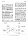
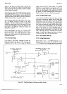
+149. BCD
REMOTE
EXPAND
0PTt0N
020
(Figure
7-3r).
4150.
0utguard
Power
Supply.
4-151.
A
microcircuit
regulator
supplies
a voltage
of
approximately +
5.3
V to
the
outguard
Data
Output,
Remote,
Trigger
and
Sample/Hold
Trigger
circuits.
This
voltage
is shown
on the schematic
diagrams
as
+
5 VI,
and is
isolated
from
all inguard
circuits.
The outguard
ground
is
also isolated
from
the
inguard
common
circuits
and
from
chassis
(earth)
ground,
and
may be floated
a
maximum
of
40 V
above
chassis
sround.
+17