76 DL-V3 User Manual Rev 3
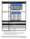
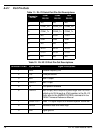
A.2.1 Port Pin-Outs
Table 11: DL-V3 Serial Port Pin-Out Descriptions
Table 12: DL-V3 I/O Port Pin-Out Descriptions
Connector
Pin No.
COM1
RS-232
COM2
RS-232
AUX
RS-232
1N/CN/CN/C
2 COM1_Rx COM2_Rx COM3_Rx
3 COM1_Tx COM2_Tx COM3_Tx
4 N/C POUT POUT
5 GND GND GND
6N/CN/CN/C
7 RTS1 RTS2 RTS3
8 CTS1 CTS2 CTS3
9N/CN/CN/C
Connector Pin No. Signal Name Signal Descriptions
1 VARF Variable frequency out
2 PPS Pulse per second
3 MSR Mark 1 output
4 EVENT1 Mark 1 input
5 PV Valid position available
6 EVENT2 Mark 2 input, which requires a pulse longer than 150 ns is
pulled up to 5V through a 47kΩ resistor in the DL-V3.
Refer also to the MARKCONTROL command in
the
OEMV Firmware Reference Manual
.
7 _RESETOUT Reset TTL signal output to an external system. Active low.
8 ERROR Indicates a fatal error when high.
9 GND Digital ground


