


3 - 15
3. SIGNALS AND WIRING
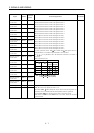
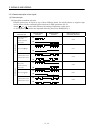
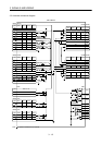
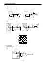
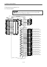
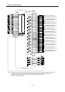
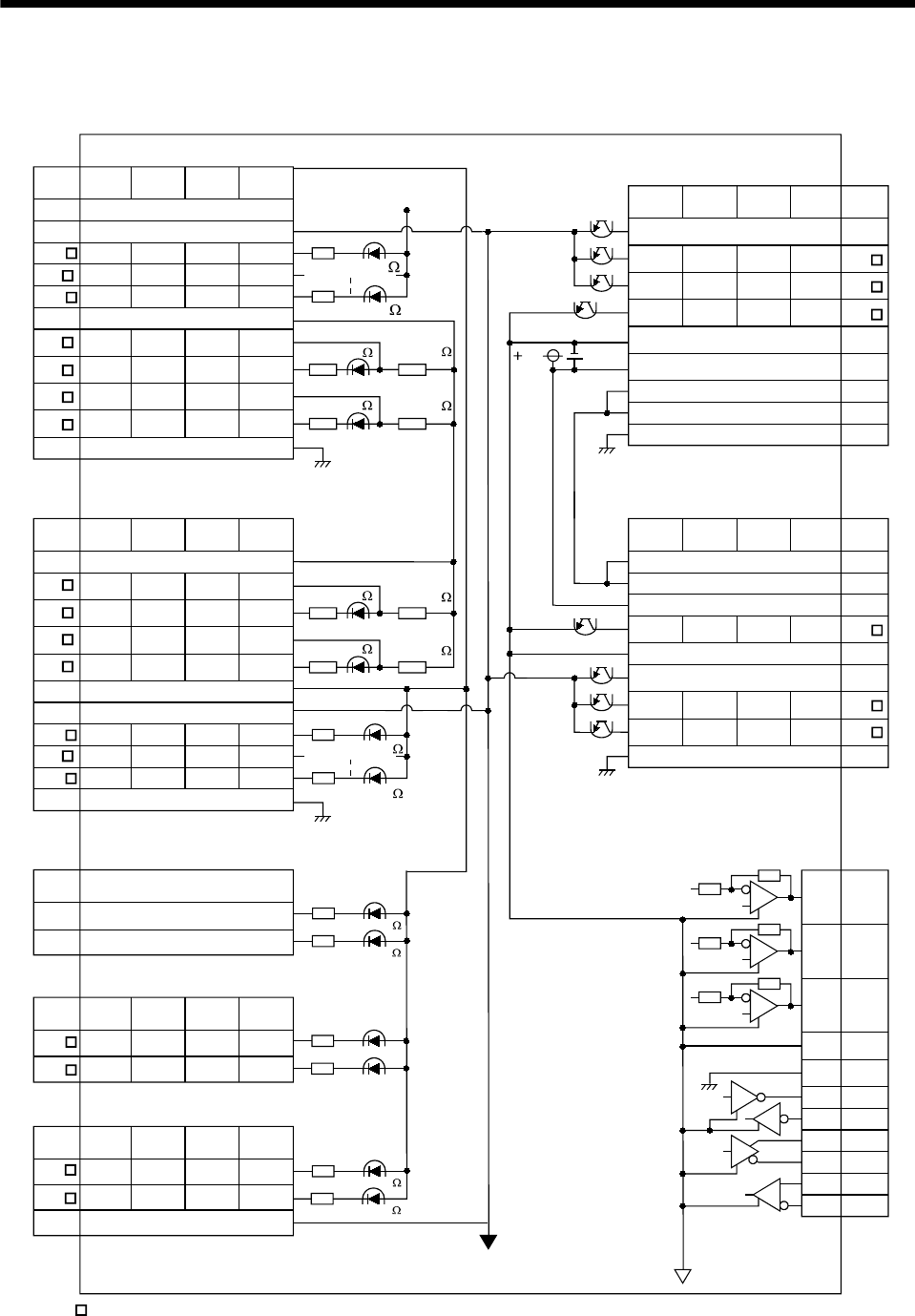
3.2.4 Internal connection diagram
SG
SDN
RDP
RDN
TXD
29
4
1
26
37
12
10
34
9
32
7
31
5
SON
CR
RES
SG
VIN
36
38
13
39
14
44
19
45
20
42
17
43
18
40
15
41
16
PG
PP
NG
NP
SD
OPC
2
38
13
39
14
44
19
45
20
42
17
43
18
40
15
41
16
PG
NG
NP
37
12
10
34
9
32
7
CR
RES
36
29
4
5
31
2
OPC
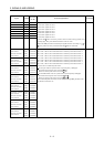
CN1A
1
MR-J2M-P8A
SG
SD
5VDC
26
VIN
SON
PP
P5
OP_COM
11
35
33
8
24
6
30
INP
OP
25
3
22
28
23
LG
SD
27
ALM_A
RD
OP_VIN
49
47
48
ALM_B
25
35
24
8
33
23
30
INP
RD
11
3
28
22
6
LG
SD
47
OP_VIN
OP
27
48
OP_COM
49
P5
MO1
MO2
MO3
LG
SD
RXD
SDP
5
12
2
9
19
15
11
7
14
4
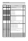
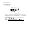
CN1A
CN1BCN1B
CN3
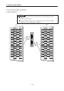
(Note)
symbol
slot 1
slot 2 slot 3 slot 4
symbol
slot 5 slot 6 slot 7 slot 8
Plate
Plate
Plate
Plate
21, 46, 50
21, 46, 50
slot 1
slot 2 slot 3 slot 4
symbol
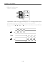
Approx.6.8k
Approx.6.8k
Approx.1.2k
Approx.100
Approx.100
Approx.1.2k
(Note)
6
LSP
LSN
1357
24 10
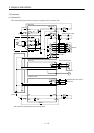
CN5
symbol
slot 1 slot 2 slot 3 slot 4
(Note)
LSP
LSN
11 13 15 17
12 14 16 18
8
CN5
symbol
slot 5 slot 6 slot 7 slot 8
(Note)
Approx.100
Approx.100
Approx.1.2k
Approx.1.2k
Approx.6.8k
Approx.6.8k
Approx.6.8k
Approx.6.8k
Approx.6.8k
Approx.6.8k
(Note)
slot 5
slot 6 slot 7 slot 8
symbol
(Note)
5V
Plate
Note. in Symbol indicates the slot number.
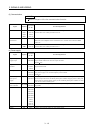
CN5
EMG_A
20
19
symbol
slot 1 to 8
EMG_B
Approx.6.8k
Approx.6.8k