


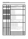
3 - 17
3. SIGNALS AND WIRING
(2) Detailed description of the interfaces
This section gives the details of the I/O signal interfaces (refer to I/O Division in the table) indicated in
Sections 3.2.2.
Refer to this section and connect the interfaces with the external equipment.
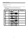
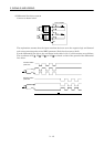
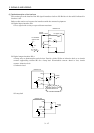
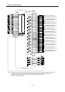
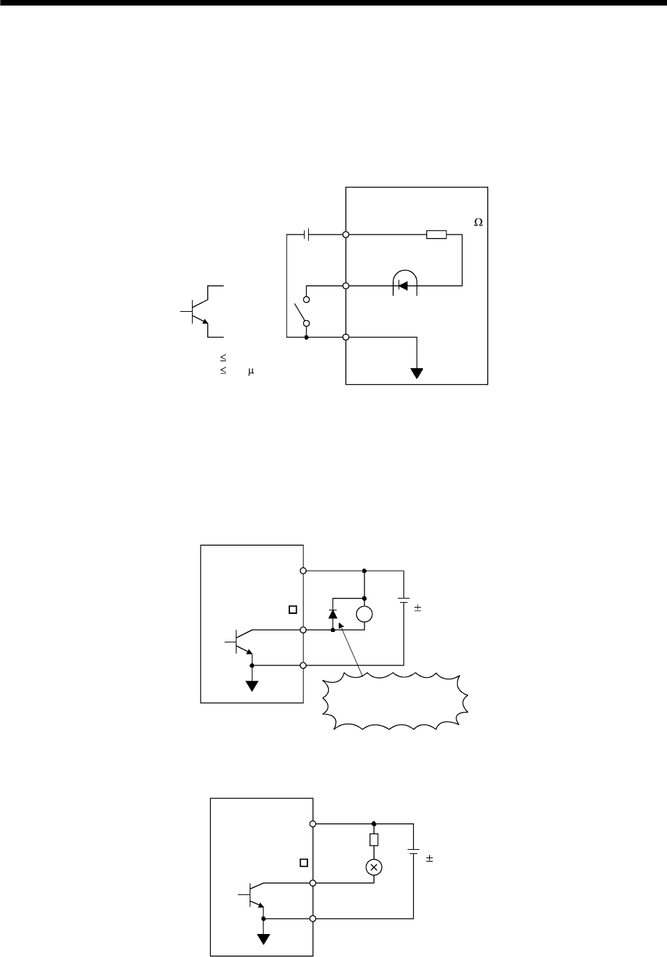
(a) Digital input interface DI-1
Give a signal with a relay or open collector transistor.
VCES 1.0V
I
CE0 100 A
Interface unit
R: Approx. 4.7k
24VDC
300mA or more
VIN
SON
etc.
SG
Switch
For transistor
Approx. 5mA
TR
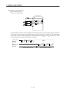
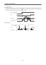
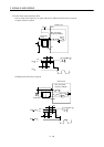
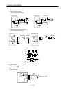
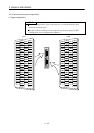
(b) Digital output interface DO-1
A lamp, relay or photocoupler can be driven. Provide a diode (D) for an inductive load, or an inrush
current suppressing resister (R) for a lamp load. (Permissible current: 40mA or less, inrush
current: 100mA or less)
1) Inductive load
VIN
SG
24VDC
10%
Interface unit
Load
Opposite polarity of diode
will fail interface unit.
ALM_
etc.
2) Lamp load
VIN
R
SG
Interface unit
24VDC
10%
ALM_
etc.