


Introduction
CPU Data Paths and Control2-2 SPRU733
2.1 Introduction
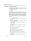
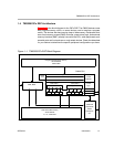
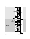
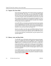
The components of the data path for the TMS320C67x CPU are shown in
Figure 2−1. These components consist of:
Two general-purpose register files (A and B)
Eight functional units (.L1, .L2, .S1, .S2, .M1, .M2, .D1, and .D2)
Two load-from-memory data paths (LD1 and LD2)
Two store-to-memory data paths (ST1 and ST2)
Two data address paths (DA1 and DA2)
Two register file data cross paths (1X and 2X)
2.2 General-Purpose Register Files
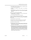
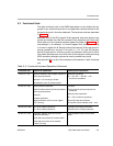
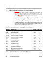
There are two general-purpose register files (A and B) in the C6000 data paths.
For the C67x DSP, each of these files contains 16 32-bit registers (A0–A15 for
file A and B0–B15 for file B), as shown in Table 2−1. For the C67x+ DSP, the
register file size is doubled to 32 32-bit registers (A0–A31 for file A and B0–B21
for file B), as shown in Table 2−1. The general-purpose registers can be used
for data, data address pointers, or condition registers.
The C67x DSP general-purpose register files support data ranging in size from
packed 16-bit data through 40-bit fixed-point and 64-bit floating point data.
Values larger than 32 bits, such as 40-bit long and 64-bit float quantities, are
stored in register pairs. In these the 32 LSBs of data are placed in an even-
numbered register and the remaining 8 or 32 MSBs in the next upper register
(that is always an odd-numbered register). Packed data types store either four
8-bit values or two 16-bit values in a single 32-bit register, or four 16-bit values
in a 64-bit register pair.
There are 16 valid register pairs for 40-bit and 64-bit data in the C67x DSP
cores. In assembly language syntax, a colon between the register names
denotes the register pairs, and the odd-numbered register is specified first.
The additional registers are addressed by using the previously unused fifth
(msb) bit of the source and register specifiers. All 64-bit register writes and
reads are performed over 2 cycles as per the current C67x devices.
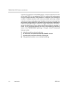
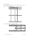
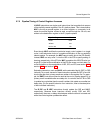
Figure 2−2 shows the register storage scheme for 40-bit long data. Operations
requiring a long input ignore the 24 MSBs of the odd-numbered register.
Operations producing a long result zero-fill the 24 MSBs of the odd-numbered
register. The even-numbered register is encoded in the opcode.
Introduction / General-Purpose Register Files