


Pipeline Execution of Instruction Types
4-21PipelineSPRU733
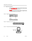
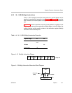
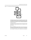
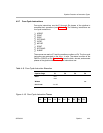
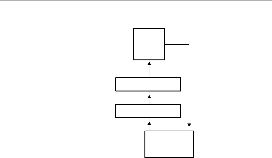
Figure 4−15. Load Instruction Execution Block Diagram
E5
Address
E3
Memory
E2
E4
Memory controller
Register file
E1
.D
Functional
unit
Data
In the E4 stage of a load, the data is received at the CPU core boundary. Finally,
in the E5 phase, the data is loaded into a register. Because data is not written
to the register until E5, load instructions have four delay slots. Because pointer
results are written to the register in E1, there are no delay slots associated with
the address modification.
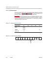
In the following code, pointer results are written to the A4 register in the first
execute phase of the pipeline and data is written to the A3 register in the fifth
execute phase.
LDW .D1 *A4++,A3
Because a store takes three execute phases to write a value to memory and
a load takes three execute phases to read from memory, a load following a
store accesses the value placed in memory by that store in the cycle after the
store is completed. This is why the store is considered to have zero delay slots.