


Performance Considerations
Pipeline4-62 SPRU733
4.4.3.2 Memory Bank Hits
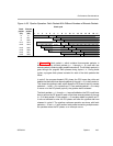
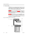
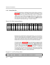
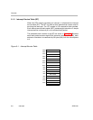
Most C67x devices use an interleaved memory bank scheme, as shown in
Figure 4−33. Each number in the diagram represents a byte address. A load
byte (LDB) instruction from address 0 loads byte 0 in bank 0. A load halfword
(LDH) instruction from address 0 loads the halfword value in bytes 0 and 1,
which are also in bank 0. A load word (LDW) instruction from address 0 loads
bytes 0 through 3 in banks 0 and 1. A load double-word (LDDW) instruction
from address 0 loads bytes 0 through 7 in banks 0 through 3.
Figure 4−33. 8-Bank Interleaved Memory
16N 16N 16N 16 N 16 N 16N 16 N 16N 16N 16 N 16N 16N 16N 16N 16N16N
0
1
16 17
Bank 0
2
3
18 19
Bank 1
4
5
20 21
Bank 2
6
7
22 23
Bank 3
8
9
24 25
Bank 4
10
11
26 27
Bank 5
12
13
28 29
Bank 6
14
15
30 31
Bank 7
+++++++++++++++123456789011112131415
Because each of these banks is single-ported memory, only one access to
each bank is allowed per cycle. Two accesses to a single bank in a given cycle
result in a memory stall that halts all pipeline operation for one cycle, while the
second value is read from memory. Two memory operations per cycle are
allowed without any stall, as long as they do not access the same bank.
Consider the code in Example 4−2. Because both loads are trying to access
the same bank at the same time, one load must wait. The first LDW accesses
bank 0 on cycle i + 2 (in the E3 phase) and the second LDW accesses bank 0
on cycle i + 3 (in the E3 phase). See Table 4−41 for identification of cycles and
phases. The E4 phase for both LDW instructions is in cycle i + 4. To eliminate
this extra phase, the loads must access data from different banks (B4 address
would need to be in bank 1). For more information on programming topics, see
the TMS320C6000 Programmer’s Guide (SPRU198).
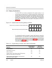
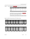
Example 4−2. Load From Memory Banks
LDW .D1 *A4++,A5 ; load 1, A4 address is in bank 0
|| LDW .D2 *B4++,B5 ; load 2, B4 address is in bank 0